
ASML and TSMC set a long runway for larger High-NA photomasks
Bottom lineThe companies target a 12-inch mask pilot line in 2031 and production-system readiness in 2033. The initiative addresses manufacturing economics years beyond the current chip cycle.

What was announced
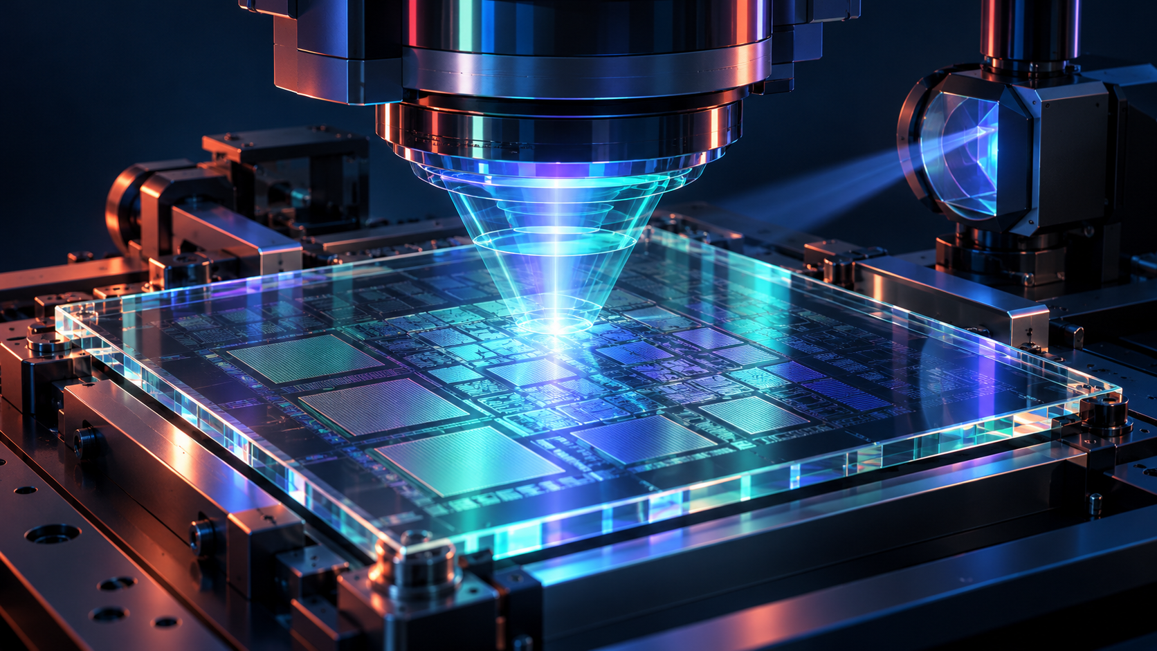
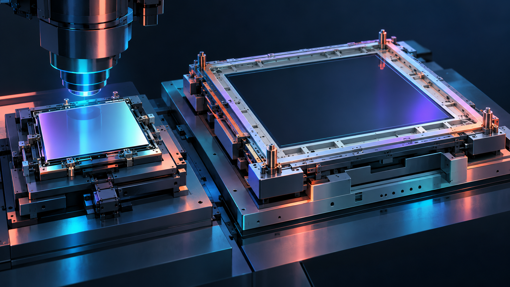
ASML and TSMC announced on September 8 that they had formed an industry initiative the previous day to move High-NA extreme-ultraviolet lithography toward 12-inch photomasks. Their targets are a mask pilot line by 2031 and systems ready for advanced-node production by 2033.
The companies say larger masks should improve productivity, lower manufacturing costs and remove stitching constraints. Their statement also says High-NA production will initially use existing 6-inch masks. TSMC separately intends to begin using ASML’s High-NA technology in high-volume manufacturing for advanced nodes in 2030. These milestones describe related but distinct phases of a roadmap.
The initiative concerns photomasks used in the lithography process. The 12-inch dimension should not be confused with a new announcement about wafer diameter. Neither the announced pilot schedule nor the projected economic benefits constitute evidence of a completed production transition.
FUVISIGHT analysis
The long schedule is part of the story. A manufacturing change can be attractive in principle and still require years of coordinated work before it is economical at scale. For a chip producer, a better process must fit a chain of equipment, materials, verification steps and operating procedures. Improving one stage while leaving another unprepared could limit the benefit to the whole factory.
The distinction between the initial High-NA deployment and the later mask transition is especially important for roadmap interpretation. Buyers should avoid treating one date as a universal switch for an entire process generation. A useful manufacturing plan can adopt a technology selectively and extend its use as supporting capabilities mature. That leaves room for several approaches to coexist.
For AI hardware developers, the potential relevance is the cost and practicality of manufacturing future designs. But the initiative is too early to support a credible forecast of cheaper accelerators on a particular date. Final economics would depend on yields, equipment utilization, design choices and the costs of the wider process. An intended productivity gain does not translate automatically into the same percentage change in a finished chip’s price.
What to watch
Watch for concrete participation from the mask and equipment supply chain, common specifications and demonstrations that move beyond an agreed objective. Later, pilot-line results should show repeatability and workable production economics. Progress is best assessed against those intermediate milestones rather than a distant completion date alone. The announcement matters because it aligns influential companies around a shared manufacturing problem; the evidence of success will come from the coordinated system they can actually build.
References
- ASML and TSMC Announce Initiative to Pioneer Industry Transition to Large-Format Photomasks for High NA EUV · September 8, 2026
- ASML and TSMC joint announcement distributed by GlobeNewswire · September 8, 2026, 02:04 ET
- ASML lines up Intel, TSMC and Samsung behind 12-inch masks — TSMC alone sets a timeline · September 8, 2026